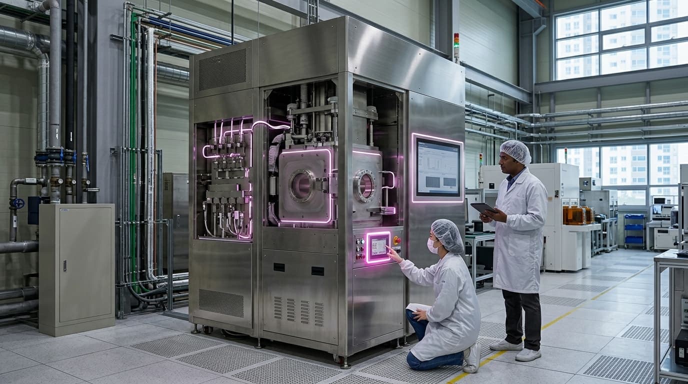
Semiconductor Equipment Localization
Geography: Asia Pacific · East Asia · South Korea
Korean semiconductor equipment companies — Semes (Samsung subsidiary), WONIK IPS, TES, PSK, and Jusung Engineering — are developing domestic alternatives to the Dutch, American, and Japanese equipment that Korean fabs depend on. The government's semiconductor equipment localization program targets 30% domestic sourcing by 2030, up from roughly 20% today. Focus areas include etch systems, chemical vapor deposition, atomic layer deposition, and metrology tools.
The urgency for equipment localization intensified after US export controls on China demonstrated how equipment supply chains can be weaponized. Korea's semiconductor industry runs on ASML lithography, Applied Materials etch/deposition, Lam Research etch, and Tokyo Electron coating/developing tools. Any disruption to these supply chains would halt Korean chip production within weeks.
Semes, as Samsung's captive equipment subsidiary, has the advantage of guaranteed demand and intimate knowledge of Samsung's process requirements. WONIK IPS is the most advanced independent Korean equipment maker, with ALD (atomic layer deposition) tools already qualified at Samsung and SK Hynix fabs. The localization effort won't replace ASML's EUV lithography (that moat is too deep), but it can reduce vulnerability in deposition, etch, cleaning, and inspection — tools where Korean companies can realistically compete.
Research this in Signals
Signals turns a topic into a sourced research record you can inspect and rerun. Your first scan is free, and this one starts with Semiconductor Equipment Localization already loaded, so edit it or scan as is.